
In the 19th century, Netherland’s cryptographer, Auguste Kerckhoff, created Kerckhoffs’s principle, stating that “A cryptosystem should be secure even if everything about the system, except the key, is public knowledge.”
Introduction
In the 19th century, Netherland’s cryptographer, Auguste Kerckhoff, created Kerckhoffs’s principle, stating that “A cryptosystem should be secure even if everything about the system, except the key, is public knowledge.” The most crucial element in chip security is the Root Key or Hardware Unique Key (HUK). The key is the starting point not only for protecting each chip but also the chain of trust that encompasses the entire system and associated services. Therefore, key generation, along with its storage and usage, must be well considered from the beginning of the design.
With the invention of Physical Unclonable Functions (PUF), we can now create a unique, inborn, unclonable key at the hardware level. The natural follow-up question to this is, “but how do we protect this key?” It is like storing your key to secrets in a drawer, a surefire way to break the secure boundary and create vulnerabilities. Security is only as strong as the weakest link, and in most cases, the weakest link is insecure key storage in eFuse. Insecure storage immediately compromises the whole system’s security, regardless of the sophistication of the key itself.
Furthermore, we know users can update the software after production, but hardware cannot be. Therefore, it is very crucial to deploy appropriate hardware security at the beginning. PUFrt, an integration of PUF and anti-fuse-based secure One-Time Programmable (OTP) memory, provides proper hardware security at the manufacturing stage. It delivers an unclonable key and secure OTP storage with complete anti-tamper designs.
↓↓↓ 5-minute video for a quick digest of this article (English voice-over + Chinese subtitles)↓↓↓
The Risks from eFuse Key Storage
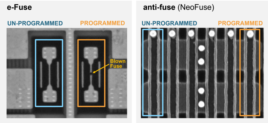
The eFuse (electronic fuse) and anti-fuse OTP memory are the most common options for key storage in modern chip design. With eFuse, the key is programmed into OTP memory by blowing a portion of metal or poly, which leaves a visible trace. Meanwhile, the anti-fuse OTP is programmed based on the oxide burn-out mechanism. The burnout creates a conductive path without a visible trace on the surface. Figure 1 shows SEM’s top view (Scanning Electron Microscope) comparison between eFuse and anti-fuse OTP after being programmed. The “0” and “1” data is stored in eFuse are easily recognizable as there is a clear opening in the cell programmed to “1”. As seen in the right image of Figure 1, the anti-fuse OTP cells look the same regardless of the data stored.
Insecure Storage Vulnerabilities
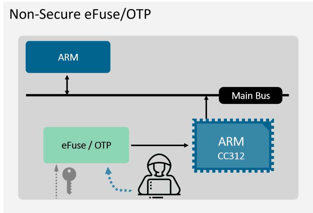
ARM core with Crypto Cell-312™ (CC312) is one of the most common design combinations found today. While all designers value the security functions provided by CC312, key storage is often overlooked. Typically, ARM CC312 is used with eFuse/anti-fuse without additional protections for key injection and storage, as shown in Figure 2. Therefore, the key remains outside the secure boundary creating a potential breach point for attackers. The problem is twofold: 1) data stored in eFuse is easily visible, as previously discussed, and 2) data can be obtained easily when access privilege control is not included. So anyone could request the secret stored in OTP. While CC312 is considered a well-designed door lock, using insecure key storage is like just leaving the key in the door lock for anyone to open the door.
Anti-tamper Enhanced Security
While the data visibility problem in eFuse can be easily solved by using anti-fuse OTP, It is still insufficient when it comes to security. Access privilege control must also be considered in the OTP controller design to enable identity differentiation and grants accessibility of secret data to authorized users only.
To further protect anti-fuse OTP in chip design, an anti-tamper design needs to be incorporated. By being in the form of physical layout, digital RTL, or a combination of both, the anti-tamper designs form a shell to counter various types of attack, such as to scramble the data when it is being written, to have glitch detection circuitry, and so on. We will discuss the topic of anti-tamper design in more detail in a future whitepaper.
Completing the Secure Boundary with PUFrt
Combining anti-fuse OTP, a controller with access privilege, and an anti-tampered shell establishes a secure Hardware Root of Trust (HRoT) countering all the discussed vulnerabilities. With a well-designed anti-tampered shell and privilege-based dual-APB interface, the secure RoT complements secure subsystems like CC312 to complete the secure boundary for the chip design. To accommodate CC312 and other ARM users, PUFsecurity developed a customized IP solution for ARM users called “Dual-APB PUFrt.” Figure 3 provides a more detailed illustration and its features.
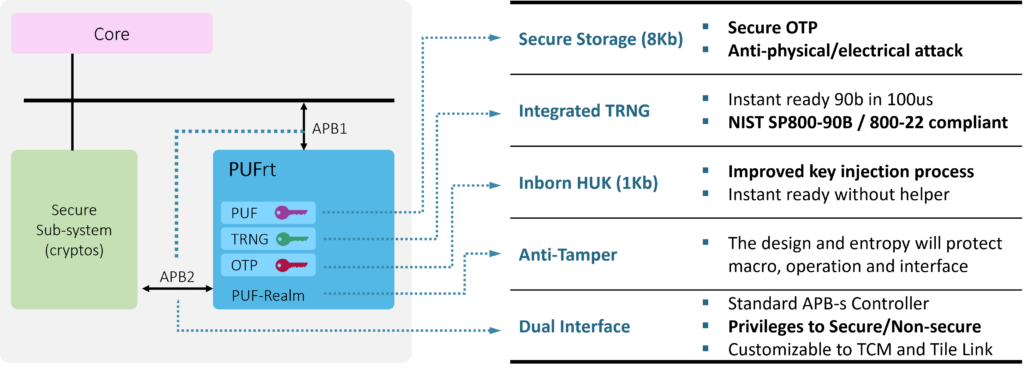
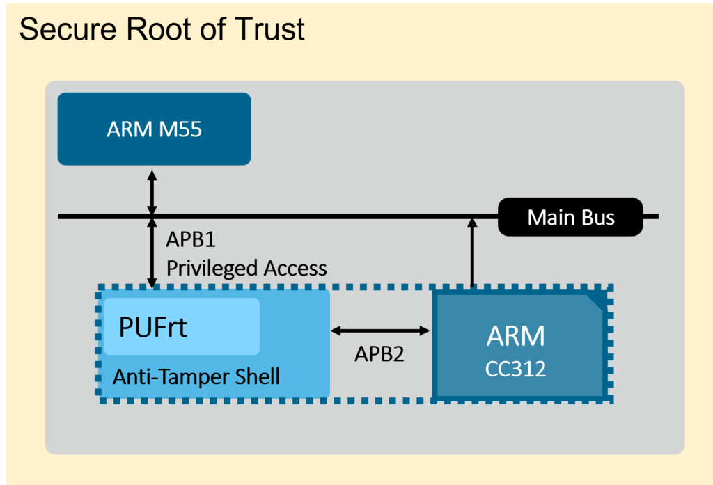
PUFrt builds upon eMemory’s anti-fuse OTP (NeoFuse) and Quantum Tunneling PUF (NeoPUF) technologies to provide self-encrypted anti-Fuse OTPwith on-chip PUF. The inborn HUK utilizes the NeoPUF’s guaranteed randomness to obtain the unique key per device, avoiding the need for a provisioning process. The True Random Number Generator (TRNG) has both digital and analog designs, combining static and dynamic entropy sources for its superb performance. PUFrt also obfuscates data and addresses and adds various security protection designs with physical/digital comprehensive tamper-proof features in an anti-tamper shell to fully protect the secret key. PUFrt is also equipped with a controller of permission control and two APB interfaces. Figure 4 illustrates an example use case of the Hardware Root of Trust IP, PUFrt, with ARM core and CC312. APB1 connects PUFrt to the main bus and enables OTP testing with JTAG, and APB2 fully integrates PUFrt into CC312 to provide secure storage and entropy source for the crypto functions in CC312. APB1 would be disabled after testing, so the secure boundary remains intact.
Dual APB PUFrt makes integration with CC312 frictionless and provides complete anti-tampering protection for key storage. In addition, the TRNG provides high-quality entropy for CC312 to perform other security functions. By integrating CC312 and PUFrt, the ARM Cortex-M55 can realize the security Root of Trust, secure storage, and security systems before being brought to the market. And such a use case applies to multiple sectors from AIoT to HPC and beyond.
Conclusion
When it comes to chip security, designers often turn to crypto subsystem solutions like ARM Crypto Cell 312. The remained obstacle, however, is how to generate and safely store the root key for the system. The dual APB PUFrt is the exact missing piece for the puzzle. With the inborn chip fingerprint from PUF that acts as a secret key to encrypt anything stored, the equipped anti-tamper shell makes it more resilient against potential attacks. With its well-planned architecture, PUFrt can be easily dropped in to replace eFuse while saving engineering effort as the controller is included. The combined solution not only completes secure boundary for IC but also maximizes the effectiveness of CC312 for the entire SoC’s performance.
Download this white paper ↓↓↓
PUFrt has a free evaluation version available for users who would like to try the IP, click here!