In my previous article, I have briefly introduced the physics of the quantum tunneling behavior in NeoPUF. In this article, I will explain, in detail, the quantum-tunneling mechanism in the gate oxide of MOSFET in advanced silicon processes and how it applies in the creation of NeoPUF characteristics.
I will use a two-dimensional cross section of a silicon dioxide atomic structure and a corresponding energy band diagram to explain trap-assisted electron tunneling.
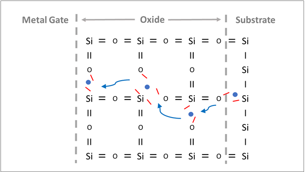
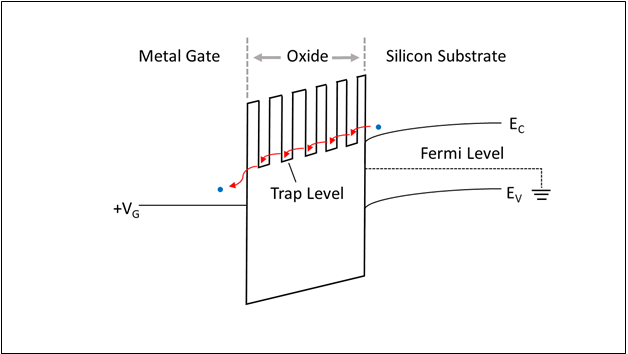
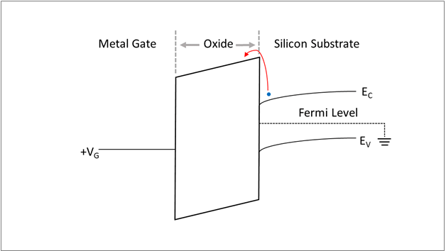
Figure 1 illustrates electron transport across silicon dioxide, from a silicon substrate to a metal gate. If there are many dangling bonds (either silicon dangling bonds or oxygen dangling bonds), due to quantum tunneling, an electron has a high probability of hopping from one dangling bond to another dangling bond, which contributes to electrical current. Whereas, as shown in Figure 2, in a structure with no dangling bond, an electron has a very small chance of jumping from a silicon substrate to a metal gate. The corresponding electron potential band diagram of metal-oxide-semiconductor of Figure 1 can be represented as seen in Figure 3.
As an electrical field is applied between the metal gate and the substrate, the electrons from the substrate can tunnel through the trap levels (dangling bonds) and transport to the gate. While the electron potential band diagram is illustrated in Figure 4, due to the lack of trap levels (dangling bonds), an electron in the substrate has to overcome a very high energy barrier to jump to the gate. Therefore, the conduction current in both cases will be very different. However, the difference in their microstructures is not possible to detect or trace physically by any means.
NeoPUF, a quantum-tunneling PUF, is formed by applying identical high electrical fields to a pair of adjacent MOSFETs that have variations in their oxide quality. Under the same voltage, an oxide that has more dangling bonds (worse quality) will be subjected to larger impact ionization by the electrons which are heated through an electronic field. These result in the generation of more dangling bonds as compared to an oxide with fewer initial dangling bonds. As the tunneling current flows through the oxide that has more dangling bonds at the sensing level, the PUF formation process ceases.
By using every two adjacent MOSFETS to repeat the process as above, a block of unpredictable and random numbers will be created because it is impossible to know which of two adjacent MOSFETs has a better oxide quality.
Once this formation is done, the set of random numbers is very reliable since the dangling bonds cannot be modified unless high temperature (> 600 degrees Celsius) is applied. It will not be affected by variations in the environment such as noise, temperature and voltage variations, since these cannot modify the dangling bonds.
The stored data “1” and “0” depend on the tunneling current. Because there are no charges stored on the device, after the power is turned off, the PUF derived from this technique cannot be physically traced.
NeoPUF and its formation mechanism, quantum tunneling, have been proven in many processes at major silicon foundries. For those who are concerned about the security of their products and want to have high quality PUF-based security solutions, NeoPUF is proven in world-leading foundries to meet your security needs.
In my next article, I will describe the characteristics of NeoPUF and quantum tunneling PUF, including their uniqueness, randomness, reliability and non-traceability, following fabrication in major foundries.