
As the first step in establishing any cybersecurity ecosystem, the process of key generation must remain reliably secure. Software-based key generation algorithms introduce various risk factors into the process, such as key management and key injection, along with the added costs required to support such processes. Thus, the safest solution is the simplest, generating an inborn root key at the hardware level through the use of a built-in PUF. There are many physical processes upon which a PUF can be built (over 40 to date), but one stands out above the rest, based on the mechanism known as Quantum Tunneling.
The Quantum Tunneling Mechanism
The transistor has an oxide layer in the gate that acts as an insulating layer which cannot conduct current. However, there are still traps caused by naturally occurring bond breakage residing in the oxide layer, which may degrade its insulating property.
Typically, there are very few traps in the gate oxide right after manufacturing. However, additional traps will be created once the gate oxide is subjected to high voltage stress. These new traps will occur randomly, with some aligning in such a way to form a conduction path through the gate oxide.
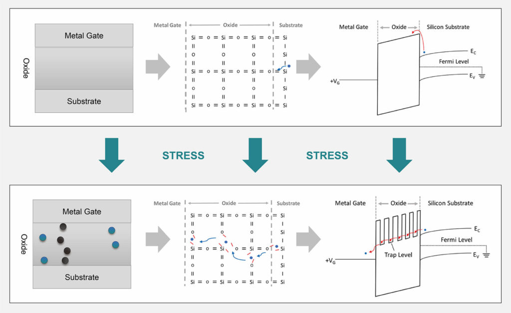
Charged carriers are more likely to be captured by these traps, and the energy barriers will be lowered at these positions. When the traps form aligned quantum wells, the charged carriers have a higher probability of tunneling through the oxide layer and causing a quantum tunneling current.
This path is permanent once created and impossible to remove, unless the oxide is annealed at a very high temperature (well above any device’s normal operating condition).
Once one of the transistors (of the transistor pair) has established a quantum tunneling path, the conducting current will automatically lower the stress voltage seen by the other transistor. This prevents the twin transistor from also establishing a second quantum tunneling path. Consequently, when reading an enrolled PUF array, we will only be able to measure current at only one of the transistors (of the pair), resulting in a highly stable PUF operation.
Enrollment
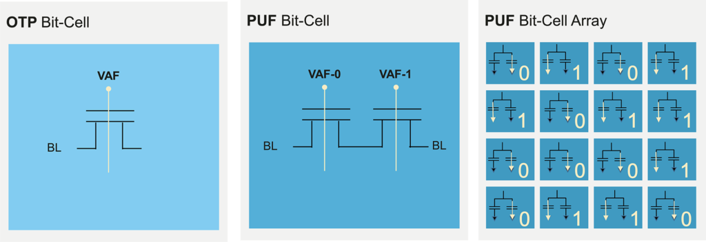
The Quantum Tunneling mechanism consists of two parallel Secure OTP bit-cell NMOS transistors. Prior to being used as a PUF, they first need to be enrolled by applying high voltage stress on the gate oxides of the two transistors.
During enrollment, one transistor will start to form a conduction path as a result of the tunneling mechanism, due to microscopic differences between the two gate oxides. Once a conduction path starts to form, the stress is released from the other oxide, assuring that only one tunneling path will be formed in a pair of transistors (either the left or right one). We can define the two different cases (left or right conduction path) as a binary one or zero.
After enrollment, the PUF can be read by sensing the current flow through each bit cell. Thus, by building a PUF with an array of such bit-cell pairs, we have the randomness needed to construct a secret data pattern upon which a device’s unique identification is based.
A Quantum Tunneling PUF achieves state-of-the-art robustness, provides 100% stable data at all possible operating conditions, and is resilient to aging effects. It also achieves this near-ideal behavior without requiring additional data processing steps, helper data, or algorithms, which are common with other types of commercially available PUFs.