
It seems that almost weekly, the semiconductor industry’s all-encompassing barometer, Moore’s Law, is pronounced dead, dying, or actually healthier than ever. As the debate continues to speculate on its health, there is an unequivocal certainty that singular monolithic chip designs are simply becoming unsustainable as FinFET technology replaces a larger slice of the traditional 2D planar gate market.
The Day of Reckoning
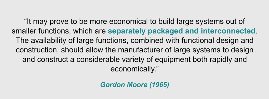
An increasing number of companies are reviving the “System in Package (SiP) or “Heterogeneous Integration (HI)” approach by fabricating standardized “Chiplets” and, from them, assembling a series of more complex designs. This modular approach of LEGO-like pieces of silicon combined into a single packaged device is nothing new and has been around since the 1980s with MCMs. Even Gordon Moore’s original essay acknowledged that a day of reckoning would come for his theory and that a more lateral approach would be needed.
Why Now for Chiplets?
Chiplets offer a flexible, scalable, and cost-effective approach that can match the ever-changing complexity of demands on modern systems.
Compared to an SoC’s more homogenous single-die integration, this heterogeneous approach can dramatically reduce fabrication and design costs, as not all chiplets would necessarily need to be fabricated on the latest nodes. For example, core logic chiplets may utilize the latest and greatest from a top-tier fab, while I/O chiplets can be produced in a smaller, more affordable foundry. So, SiPs can offer substantial benefits over single-die SoCs, such as higher wafer yields and a faster time-to-market, despite the complexity of integrating them into a single package with a specialized chiplet substrate (the interposer layer).
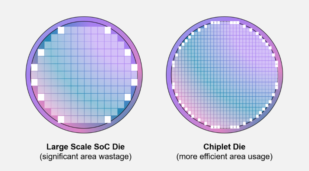
As the feature size for each advancing process node reduces, there is a corresponding trend of increased defect density, presenting a significant problem for the manufacturer. Combined with the larger absolute size of complex SoC designs, there are significantly fewer usable good dies per wafer for large monolithic designs. If the defect density continues to grow as we push further and further towards sub-nanometer technology, what choice is left but to decrease the size of the dies themselves?
Yields, however, can be improved by producing smaller designs (chiplets) to be assembled into a larger design (SiP). Another benefit is better wafer utilization, which is achieved by packing more chiplets per wafer than a die of large SoCs, which wastes a significant amount of space.
Chiplet Implementation Today
The system’s flexibility means that only the chiplets corresponding to the update in function require a redesign, minimizing the overall workload of a design transitioning to a newer node. The cost savings can also be passed along the supply chain, removing the need for a separately designed product family targeting different markets. This simplifies stock-keeping unit (SKU) costs by substituting the appropriate chiplet to match the targeted market segment in price and performance.
Given the benefits of chiplet-based design, it comes as no surprise that many industry heavyweights have started their chiplet programs: Intel with their Agilex FPGAs and SoCs, AMD and their EPYC and Ryzen processor families, Nvidia using their chiplet interconnect technology NVLink-C2C, and even TSMC in 2020 when they introduced their 3DFabric technologies to help customers design their own chiplet-based SiPs. Not to miss out on the action, the US government has also put resources into exploring this promising style of chip design with DARPA’s Common Heterogeneous Integration and Intellectual Property Reuse Strategies (CHIPS). Finally, demonstrating that chiplet-based design is not just a passing fad, there is already a push for formalizing the way chiplets talk to each other, with the Universal Chiplet Interconnect Express (UCIe) open standard being promoted by companies such as Intel, AMD, Arm, TSMC, Samsung, Qualcomm, Google, and Microsoft.
Security Implications
As prevailing trends favor a chiplet-based approach over a monolithic single-die SoC, we will likely have upwards of ten chiplets, each potentially from different wafers, integrated into a single design. From a security viewpoint, the number of attack surfaces will rapidly multiply when moving from one single SoC die to multiple dies for SiP. Each chiplet procured has numerous possible foundry sources and design companies involved. Not only are there multiple sets of I/Os to protect, but each vendor will not necessarily adhere to the same set of security protocols.
Currently, this may not be a concern, as chiplets only take a small market share. However, as chiplets begin to see wider adoption, the number of chiplet vendors will expand, and managing the different security conventions will quickly become a significant risk.
The Chiplet Supply Chain Risk
The geopolitical tensions that link vendors internationally only add to the complexity, especially as tensions between the US and China continue to rise, each seeking to bifurcate the already fragile semiconductor supply chain. Therefore, safely tracing the components through the supply chain from one location to the next is crucial for securing SiPs. Therefore, any potential weak link in the supply chain presents a ripe target for an adversary to insert a compromised chiplet, possibly with a malicious payload, trojan, or spyware.
PUF Chip Fingerprinting
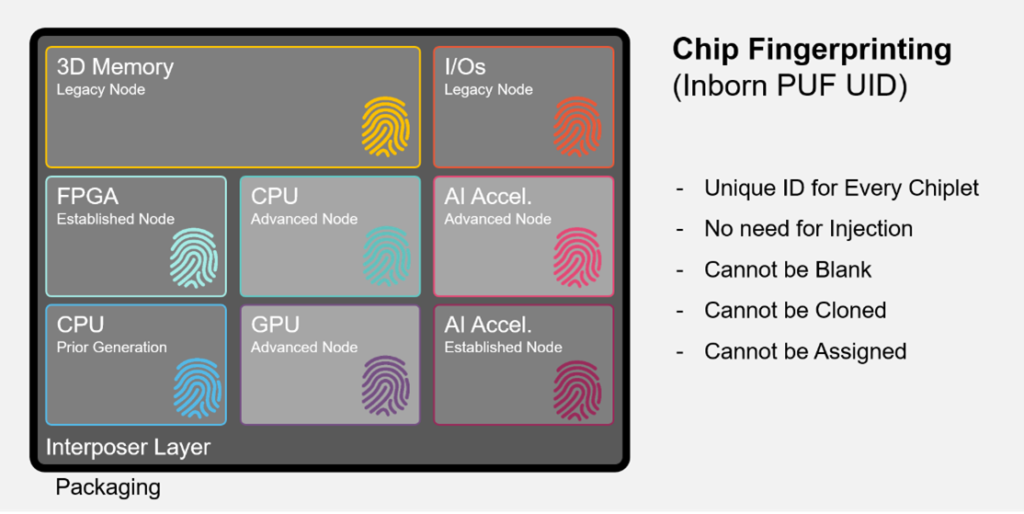
Given these new security challenges being faced during this transition to chiplet-based architecture, it is reassuring to know that the same PUF protection currently deployed with SoCs can also create a foundational root of trust for SiPs. When integrated into the design, they can provide each chiplet with a Unique Identity (UID) derived from a PUF Chip Fingerprint.
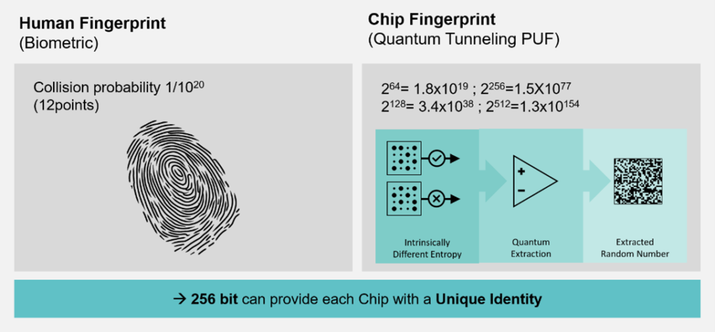
A physically unclonable function (PUF) embedded into every chiplet in a SiP will bring together the fragmented nature of chiplet-based design and support the four central security functions.
- Authentication: By identifying each chiplet, PUFs will make it possible to ensure that every chiplet is genuinely sourced from a legitimate supplier.
- Provisioning: After verifying that each chiplet is authentic, the central security server may turn it on preventing counterfeit or tampered chiplets from entering the supply chain through unauthorized channels. Provisioning can also be used to turn on and off features in a system, tailoring each design to a specific market or target customer while using the same base SiP for these different cases.
- Tracking: When each chiplet has a unique identifier, tracing them throughout the design and assembly process becomes a much easier proposition. Leaving a clear audit trail through the SiP supply chain is especially important to customers where a security breach could have disastrous consequences, such as in the automotive or aeronautic markets.
- Analysis: When we are able to identify each chiplet, we can receive feedback on the status of each one. This data can be sent back securely for real-time analysis, failure analysis, or even continuous status monitoring for mission-critical applications that cannot afford downtime.
Granted, each chiplet may be provisioned separately with its own ID through an external key injection process but given the number of chiplets that will go into a complex design, it would make much more sense to do this automatically through embedding a PUF capable of internal key provisioning without the need for a secured, clean room environment and associated security hardware required for the generation of unique IDs.
Supporting the four features mentioned above can be attained easily by adding a PUF to each chiplet in an HI design. Alternatively, if one of the chiplets was dedicated solely to security, a PUF-based Chiplet Hardware Secure Module (CHSM) could be utilized. In that case, the SiP would no longer need to rely as much on an external, secure server to provide services such as the authentication process mentioned above.
With a CHSM performing similar duties that a root-of-trust performs in an SoC, the overall basis of SiP security can come from the CHSM itself. With such a basis, a “secure boot” like process may also be implemented in the SiP. This, in theory, would begin with the CHSM’s authentication, then authorizing the next chiplet in the chain to be enabled, then start the authorization process of the next chiplet in the chain, and so on until the entire SiP is brought up. Depending on how the CHSM was configured, it may also act as a security controller to monitor the other chiplets for security property violations, hardware trojans, and tampering. Adding extra sensors allows further detection of physical tampering, such as through laser, X-ray, voltage/clock glitching, and more. It is important to catch such fault injection (FI) types of attacks since they often lead to side-channel analysis/attacks.
Conclusion
Regardless of the debate around the endpoint of Moore’s Law, there is an unequivocal need for lateral innovation to counter the physical limits of smaller process nodes. And chiplet architecture will likely play a vital role in this. However, with such a radical reimagining of the design fabrication process, there will be a litany of unpredicted security issues to consider as we move from SoC to SiP.
The most likely scenario will be deploying a pre-qualified and certified PUF-based Secure Element (SE) chiplet in each 3D package. This will allow a Hardware Root of Trust to underpin the security of the data in-use, in-transit, and at-rest. As newer generations of a chip’s design are brought to market, with CPUs migrated to the most advanced processes, the same verified and qualified PUF-based SE chiplets can continue to be deployed, streamlining the process.
It’s not much of a jump to imagine a future where each chiplet in the same 3D package deploys PUF-based protection. Standardizing SiP security seems inevitable in the face of supply chain security risks and the need to safely assemble, verify and update a SiP.